Application of Laboratory Film Applicator in Semiconductor Material Moulding
introduction
Semiconductor materials play a vital role in modern electronic devices. From computer chips to smartphones, solar cells, and LED lighting, semiconductors have a wide and expanding range of applications. In these applications, coating technology plays a decisive role as one of the important processes in material preparation. As an important experimental equipment, the coating machine is widely used in the research and development of semiconductor materials. This article will discuss in detail the application of laboratory film coating machine in semiconductor material film making, including its principle, types, application cases and future development directions.
Overview of coating technology
Coating technology is a method of achieving a specific function or property by evenly covering one or more layers of functional materials on the surface of the substrate. Common coating methods include physical vapor deposition (PVD), chemical vapor deposition (CVD), spin coating, spraying, dip coating, etc. Different coating methods are suitable for different materials and applications.
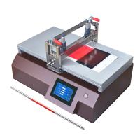
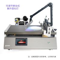
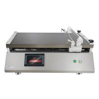
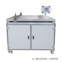
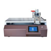
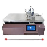
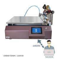
The working principle of the Film Applicator
The coating machine achieves high-quality film preparation by controlling the deposition speed, thickness, uniformity and other parameters of the coating material. Its core components include coating heads, substrate tables, vacuum systems, heating systems and control systems. According to the different coating methods, the coating machine can be divided into spin coating machine, spraying machine, evaporation machine, sputtering instrument, etc.
Types and characteristics of laboratory film coating machines
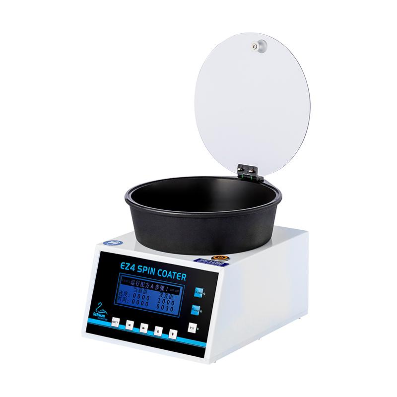
Spin Coater
The spin coating machine, also known as the homogenizer, is one of the common coating equipment in the laboratory, which is widely used in the preparation of photoresists, thin-film batteries, displays and optoelectronic devices. The working principle is to drop the coating material onto a rotating substrate and spread the material evenly through centrifugal force to form a uniform film.
Advantages of Spin Coaters:
The Spin Coater is easy to operate and is suitable for coating a variety of liquid materials.The coating film has good uniformity and controllable thickness.It can handle a wide range of substrates and can be used in a wide range of applications.
Application examples of Spin Coaters
1) Application in the lithography process: In the lithography process, the Spin Coater is used to evenly coat the photoresist on the surface of the silicon wafer to form a lithography pattern. By controlling the rotation speed and time, the thickness of the photoresist can be precisely controlled, which affects the resolution and accuracy of the pattern.
2)Preparation of OLED displays: Organic light-emitting diode (OLED) displays rely on high-quality organic thin film layers. Spin Coaters are used to coat OLED materials to ensure the brightness and color uniformity of the display.
Spraying machine
The sprayer sprays the coating material onto the substrate in atomized form through the air stream, and is suitable for coating film on substrates with large areas and complex shapes. Spraying technology includes various forms such as thermal spraying, plasma spraying, and cold spraying.
Advantages of spraying machines:
The spraying machine is suitable for large-area coating film and has high production efficiency.Capable of handling substrates with complex shapes.Suitable for a wide range of materials, including metals, ceramics, and polymers.
Application examples of sprayers
1)Preparation of solar cells: Spraying technology is used for the deposition of thin film materials in solar cells, such as perovskite layers in perovskite solar cells. The spraying method enables large-area coating and improves productivity.
2)Preparation of thermal barrier coatings: In aero engines and gas turbines, thermal barrier coatings are used to protect the base material from high-temperature corrosion. Plasma spraying technology can deposit a uniform ceramic coating on a substrate with complex shapes, improving the heat resistance of the coating.
Evaporation machine
The evaporator forms a thin film by heating the material so that it evaporates and deposits it onto the substrate in a vacuum environment. Evaporation technologies include hot evaporation, electron beam evaporation, and molecular beam epitaxy (MBE).
Advantages of evaporators
The evaporation machine can achieve high-purity, high-quality thin film preparation. moreoverIt is suitable for coating materials with high melting points.The thickness and composition of the coating film can be precisely controlled.
Application case of evaporation machine
1)Preparation of semiconductor devices: Evaporation technology is widely used in the preparation of metal contact layers and insulating layers in semiconductor devices. For example, in integrated circuits, metals such as evaporated aluminum, copper, etc., are used to form conductive interconnect layers.
2)Preparation of optical thin films: In optical devices, evaporation technology is used to prepare mirrors, filters, and anti-reflective coatings. By controlling the evaporation rate and deposition conditions, thin films with specific optical properties can be realized.
Sputter meter
The sputtering instrument bombards the target with an ion beam, causing the target atoms to sputter onto the substrate to form a thin film. Sputtering technologies include DC sputtering, radio frequency sputtering, and magnetron sputtering.
Advantages of sputtering instrument
Sputterers are suitable for coating a wide range of materials, including metals, alloys, oxides, and more.The coating film uniformity is good and the film forming speed is fast.It can be applied at low temperatures, and is suitable for heat-sensitive materials.
Application examples of sputterers
1)Preparation of hard disk films: Magnetic thin films in hard disk drives are prepared using sputtering technology. Through magnetron sputtering, high-density magnetic materials can be deposited on the substrate to improve the storage density of hard disks.
2)Preparation of transparent conductive films: In touch screens and displays, transparent conductive films (e.g., ITO films) are key materials. RF sputtering technology enables the deposition of uniform ITO films on glass or plastic substrates, ensuring good conductivity and light transmission.
Practical application of laboratory film coating machine in semiconductor material filmmaking
1. Preparation of semiconductor nanomaterials
Coating technology plays an important role in the preparation of semiconductor nanomaterials. For example, with spin coating, homogeneous thin films of quantum dots can be prepared for use in quantum dot light-emitting diodes (QLEDs) and solar cells. By controlling the coating parameters, the thickness and surface topography of the film can be precisely adjusted to optimize its optoelectronic properties.
2. Preparation of high-performance thin-film transistors
Thin-film transistors (TFTs) are the core components of devices such as displays and sensors. Using sputtering and evaporation technology, high-quality semiconductor thin films and dielectric layers can be prepared, thereby improving the electrical properties and stability of TFTs. For example, in oxide semiconductor TFTs, magnetron sputtering is used to deposit IGZO (indium gallium zinc oxide) thin films, ensuring their high mobility and stability.
3. Research on new two-dimensional materials
Two-dimensional materials such as graphene and transition metal disulfides (e.g., MoS2) show great potential in electronic devices. Coating technology enables the preparation of high-quality films for these materials. For example, by spraying technology, graphene dispersions can be uniformly coated on substrates to prepare highly conductive graphene films for use in flexible electronics and sensors.
4. Development of high-efficiency solar cells
In the development of solar cells, coating technology is used to prepare key components such as light absorption layers, electron transport layers, and electrode layers. For example, in perovskite solar cells, spin coating technology is used to deposit uniform perovskite films to ensure high photoelectric conversion efficiency. By optimizing the coating process, the stability and efficiency of solar cells can be improved.
conclusion
The application of laboratory film coating machine in semiconductor material film making has a wide prospect and important significance. By selecting the appropriate coating method and equipment, high-quality thin film preparation can be achieved, which promotes the development of semiconductor materials and devices. With the continuous progress of science and technology, coating technology will develop in the direction of high precision, intelligence, multi-function and environmental protection, and further enhance its application value in the preparation of semiconductor materials.


- 1How Flat Film Applicators Can Build a New Generation of Functional Materials on Fabrics
- 2NVP anode film FAQ and solution
- 3Application Technology of Laboratory Film Applicator in Dielectric Thin Film
- 4Comparison of Advantages and Disadvantages of Three Heating modes for Laboratory Film Applicators
- 5Application and selection of laboratory coater in PDMS thin film prepative
- 6Scraping machine selection case: film substrate large size high accuracy scraping solution
- 7Application of Laboratory Automatic Film Applicator in Coating Battery Slurry on Copper Foil and Aluminum Foil
- 8Application of Film Applicator in PEM Research and Preparation
- 9Application of Film Applicator in PVDF-HFP Material Research