Destructiveness gluing tensile test
Purpose
The purpose of this test is to measure bond strength, evaluate bond strength distribution, or determine compliance with specified bond strength requirements of applicable procurement documentation. The test can be applied to wire-to-wire bonds, wire-to-substrate bonds, or wire-to-package wire bonds within packages of wire-connected microelectronic devices bonded by soldering, thermocompression, ultrasonics, or related techniques. . It can also be applied to bonding external to the device, such as from the device terminals to the substrate or wiring board, or to the die and substrate in non-wire bonded device configurations such as bundle-lead or flip-chip devices. Internal bonding between bases.
instrument
The equipment used for this test shall include suitable equipment for applying the specified stresses to the bonds, leads, or terminals as required under the specified test conditions. Calibrated measurements and indications of applied stress in kilogram-force (gf) shall be provided by equipment capable of measuring stress up to twice the specified minimum limit with an accuracy of ±5% or ±0.3 gf, whichever is the greater tolerance.
program
The tests shall be conducted using the test conditions specified in the applicable acquisition documentation consistent with the particular device construction. All pull forces shall be calculated and, where applicable, prescribed sampling, acceptance and added sample regulations shall be followed. Unless otherwise specified, for Conditions A, C, and D, the sample size number specified for the bond strength test shall determine the minimum sample size, not the sample, based on the minimum number of bond pulls to be accomplished, except from a minimum of 4 devices Randomly select the desired number of bond pulls. Bond pulls under test conditions D, F, G and H, although involving two or more bonds, should be counted as a single pull for bond strength and sample size purposes. Unless otherwise stated, the sample size specified in Conditions F, G, and H. shall determine the number of dies (not bonds) to be tested. For hybrid or multi-chip devices (all conditions), at least 4 chips should be used or all chips should be used if 4 chips are not available on a minimum of 2 full devices. If there are any adhesives, sealants or other materials under, on or around the mold to increase the apparent bond strength, a bond strength test should be performed prior to construction. The stress required to achieve bond failure shall be observed and the physical location of the point of failure recorded as listed (see 3.2.1).
When flip-chip or beam-leaded chips are bonded to a substrate other than the finished device, the following conditions shall be met:
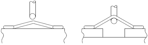
Figure 2011-3. coil angle
In addition, RF/microwave hybrid circuits containing wires that cannot be accessed by hooks need to be replicated on the test coupon in such a way as to allow entry of hooks for pull testing. These wires should be bonded at the same time the production hybrid is bonded using the same setup, operator and schedule. Test sample lines shall be subjected to pull testing in lieu of tuned or inaccessible lines for production hybrids. Failure of the test specimen shall be considered a failure of the production unit and appropriate actions shall be taken according to the applicable specification (Figure 2011-4).
Figure 2011-4. Flat Ring Pull Test
Table I. Minimum Bond Strength
failure category
The failure categories are as follows: When specified, the stress required to achieve separation and the category of separation or failure shall be recorded.
Silicon is broken.
Beam lifts on silicon.
The beam breaks.
The beam breaks at the edge of the silicon.
The beam breaks from edge to edge of the silicon.
Bond lifted.
Lift the metallization from the die (metallization separation), separating the pads.
Enhance metallization.
If applicable, the bonding material or base fails.
Fracture of the mold (or carrier) or substrate (removal of a part of the mold or substrate directly under the bond).
Lift metallization (separation of the metallization or bond pad from the die (or carrier) or substrate).
Broken leads or terminals at the point of deformation (solder affected area).
Breakage of the lead or terminal at a point not affected by the bonding process.
Bond interface failure (either in the solder or at the solder interface between the lead or terminal and the board or substrate conductor making the bond).
The conductor is lifted from the board or substrate.
Fractures in boards or substrates.
Broken wire at the point of necking (reduction of cross-section due to bonding process).
Break the line at points other than the constriction.
Bond failure on chip (interface between wire and metallization).
Adhesion failure outside the substrate, package pillar, or chip (interface between wire and metallization).
Lift the metallization from the mold.
Lift the metallization from the substrate or package pillar.
Death fracture.
Substrate breaks.
For internal wire bonding:
For external bonding that connects the device to a terminal block or substrate:
For flip chip configuration:
For beam lead assemblies:
NOTE: RF/Microwave mixers require very flat loops, which can lead to erroneous wire pull data, the following formula can be used to determine the correct wire pull value.
V 1 = V 2 sin Θ
Where:
V 1 = new value for pull-out test.
V 2 = Table I value for test size wire
Θ = maximum calculated wire loop angle (Fig. 2011-3).Test Condition A - Adhesive Peel
该测试通常用于器件封装外部的键合。引线或端子和器件封装应以这样的方式夹紧或夹紧,使得在引线或端子与板或基板之间以规定的角度施加剥离应力。除非另有规定,否则应使用90度的角度。当发生故障时,应记录导致故障的力和故障类别。
测试条件C - 拉线(单键)
该测试通常用于管芯或衬底和微电子器件的引线框架处的内部键合。连接模具或基板的导线应切割,以便提供两个可进行拉力测试的端部。在短线路的情况下,可能需要将线切割成靠近一个终端,以便在相对的终端处进行拉力测试。电线应夹在合适的装置中,并且以这样的方式将简单的拉动作用施加到电线或装置上(用电线夹紧),使得力大致垂直于模具或基板的表面施加。当发生故障时,应记录导致故障的力和故障类别。
测试条件D - 拉线(双键)
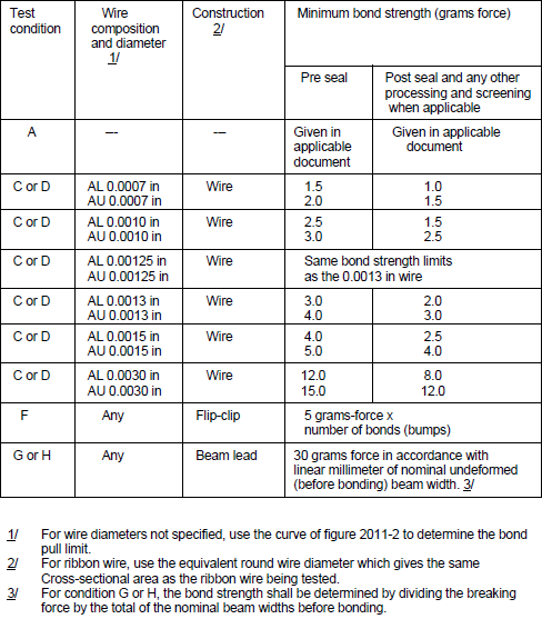
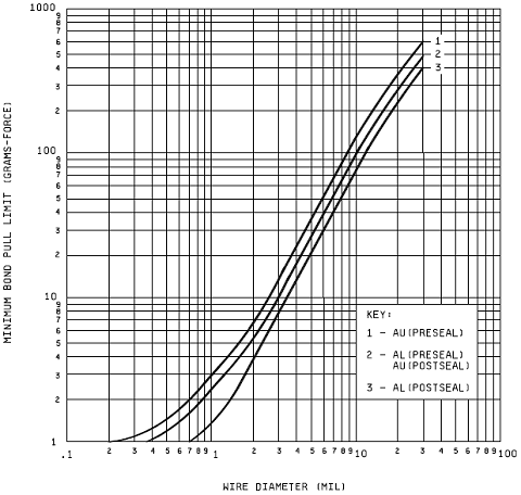
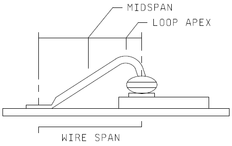
该程序与测试条件C的程序相同,不同之处在于通过在引线下方插入一个钩子(连接到模具,基板或头部或两端)来施加拉力,同时夹紧设备并钩住中跨和环之间的电线。顶点,不会引起不良的线材变形(对于正向楔形和球形结合,这将在中跨和模具边缘之间:对于反向结合,这将在中跨和包装边缘之间)并且拉力沿垂直方向施加模具或基板表面。参见图2011-1。当发生故障时,应记录导致故障的力和故障类别。最小粘结强度应从取表我。图2011-2可用于表I中未规定的线径。对于线径或等效横截面> 0.005英寸,其中钩子不能装配在线下,可以使用合适的夹子代替钩子。
图2011-1。邦德拉钩放置位置
图2011-2。最小债券拉动限制
注:最小粘结强度应采取表我。图2011-2可用于表I中未规定的线径。
测试条件F - 键合剪切(倒装芯片)
该测试通常用于半导体管芯和衬底之间的内部键合,其以面粘合的配置连接到该衬底。它还可以用于测试衬底和安装管芯的中间载体或辅助衬底之间的键合。合适的工具或楔子应在主基板正上方的位置与模具(或载体)接触,并垂直于模具(或载体)的一个边缘并平行于主基板施加力,以产生粘合剪切失败。当发生故障时,应记录故障时的力和故障类别。
测试条件G - 推出测试(梁引线)
该测试通常用于过程控制,并用于粘合到特殊制备的基板上的半导体芯片样品。因此,它不能用于生产或检验批的随机抽样。应采用含孔的金属化基板。适当居中的孔应足够大,以便为推动工具提供间隙,但不足以干扰粘合区域。推动工具应足够大,以尽可能地减少测试期间的器件开裂,但不足以接触锚固区域中的梁引线。按如下方式进行推进试验:基板应牢固地固定,推动工具通过孔插入。推动工具与硅器件的接触应该没有明显的影响(小于0.01英寸/分钟(0。254毫米/分钟)并以恒定速率压在粘合装置的下侧。当发生故障时,应记录故障时的力和故障类别。
测试条件H - 拉断测试(梁引线)
该测试通常在样品基础上用于束引线装置,该束引线装置已经粘合在陶瓷或其它合适的基底上。校准的拉出装置(见2)应包括一个拉出杆(例如,镍铬合金或可伐合金线的电流回路),以与硬固化粘合剂材料(例如,热敏聚乙酸乙烯酯树脂胶)连接。在梁引线模的背面(顶侧)。基板应牢固地安装在拉出夹具中,拉出杆应与粘合材料牢固地机械连接。该装置应在法线的5度范围内拉至至少计算出的力(见3.2),或直到模具在基板上方2.54毫米(0.10英寸)处。当发生故障时,应记录故障时的力,计算的力限制和故障类别。
钢丝球粘合剪
按照JEDEC JESD22-B116线焊剪切试验方法的程序。
测试条件:
失败标准
在施加的应力下分离的任何粘合拉力小于表I中所示的作为所示试验条件,组成和结构所需的最小粘合强度的粘合拉力应构成失效。
用于该测试的芯片样本应从与它们要表示的已完成设备中使用的相同芯片群中随机获取。
在完成的器件粘合的时间段内,用于该测试的芯片应与完成的器件粘合在同一粘合设备上。
在完成的器件衬底处理的同一时间段内,测试芯片衬底应与完成的器件衬底相同地进行处理,金属化和处理。
概要
以下详细信息应在适用的采购文件中规定:
测试条件信(见3)。
如果不符合3.2中规定的最小粘结强度或所需强度分布的细节(如适用)。
样品尺寸编号和接受编号或编号以及每台设备上要测试的粘合拉力的选择,以及设备数量(如果不是4)。
For test condition A, if not 90°, the bond peel angle and bond strength limit (see 3.2).
Requirements for reporting separation force and failure category, if applicable (see 3.2.1).


- 1What are the common tensile test applications and standards?
- 2What is bond strength?
- 3What kind of adhesive bond strength is suitable and satisfactory?
- 4How to calculate elongation in tensile test?
- 5What are the commonly used tensile test standards?
- 6What are the common tensile testing applications?
- 73 basic types of material destructive testing
- 8Evaluation of measurement uncertainty in tensile testing
丁富连;王承忠;陈卓人;方健 - 《宝钢技术》
- 9Discuss the influence of the flexibility of the analytical testing machine on the results of the tensile test
余立; 李荣锋; 凃应宏 - 《试验机柔度对拉伸试验结果的影响》