Application of wet-film
Earlier PCB pattern transfer materials used a wet film production process, and the shortcomings of using wet film technology and PCB requirements to improve the wet film were also revealed, mainly due to the long production cycle of polyethylene, uneven coating thickness, coating board pins and debris Difficulty after developing too many films. It is more difficult to jointly control the process leading to subsequent wet film production problems, and eventually the wet and dry film is replaced.
With the development of PCB assembly technology, and the smaller and smaller PCB lines and line spacing, the accuracy and density requirements are getting higher and higher, the traditional problem in this dry PCB mode transfer process is mainly reflected in the further increase in resolution without drying (Mainly due to polyester dry coating film), which cannot meet the needs of specific PCB production, needles and substrates, pits, scratches affect the effect of the film, resulting in trachoma, gaps, and broken wires in the finished product. Wet films were advanced to address these issues, offering a way.
Characteristics of a wet film
1 adhesion, good coverage
The wet film itself is composed of photosensitive synthetic resin, photosensitizer, colorant, filler and solvent viscous blue liquid. In the pits on the substrate, the contact with the wet film is the scratch part is good, and it is mainly bonded through the action of the wet film and the substrate, so that the wet film copper foil and the substrate have good adhesion, and the screen can be obtained well Coverage, which is a high-density thin line that provides PCB processing conditions. Table I can be explained by the wet adhesion of the film:
Surface Dry, Wet Film Adhesion Test Comparison Table
Coated module shedding rate (%)
6 * 6mil 7 * 7mil 8 * 8mil 9 * 9mil
Dry 0.06
0.01 0.02 0
wet film 0000
The data in Table I show that the adhesion of the wet film is much better than that of the dry film, and fine lines are much better relative to the production of the wet film.
2 good resolution
The wet film is in contact with the substrate, and the coverage is good, and the film contact exposure is used to reduce the light path, which can reduce light loss and errors caused by light scattering. The resolution of this wet film is generally 25 μm or less to improve the precision of pattern making, where it is difficult to achieve practical resolution at a dry 50 μm.
3 low cost
The wet film thickness is controllable, generally thinner than the dry film, the packaging cost is low, and the wet film cost is relatively low. Wet film in the fine-line in-house process enables a greatly improved yield, saving 20% of the cost compared to dry materials. The speed of wet development can be increased by 30%, the etching rate can be increased by 10-20%, and the speed of fading film can be increased, so as to save energy, improve equipment utilization, and finally reduce costs.
4 Eliminate the fear of the edge of the board
It is easy to paste the edge of the dry board, and it is easy to cause the film to be broken during the production process, which will affect the board pass rate, and the edge of the board will not be printed on the wet film.
Two wet film processes
According to our own conditions, our company uses various wet films, and finally selects Beijing Rio Tinto wet film. Its internal processing procedure is as follows:
Brush plate (substrate pretreatment) → drying → screen printing → exposure → development → → thin film etching
General double-panel process:
Brush plate (substrate pretreatment)→drying→screen printing→exposure→development→electroplating→etching film formation
There are three operating points when applying wet film
1 brush board
The material provided by the former process (i.e. the production board) requires that the board has no serious oxidation, oil stains, and creases. We spray with acid (5% sulfuric acid) to remove organic impurities and inorganic pollutants, and then grind with 500 mesh nylon brush roller. Brush plate realization: no copper oxide on the surface, uniform and rough copper surface, strict smoothness of copper surface, and water marks on copper surface. This effect increases the bond strength between the wet film and the copper foil surface to meet the requirements of subsequent process steps. The surface condition of brushed copper foil after PCB directly affects the yield.
2 screen printing
In order to select the desired wet film thickness prior to printing the screen, attention is paid to the thickness of the mesh (i.e. the number of lines per unit length) of the grid. With the same amount of ink film thickness on the screen, the theoretical ink volume (Uth) through the ink is as follows:
Uth = Dw2\(w+d)2×1000
(D─clean sand thickness d─diameter w─opening width)
The actual ink volume is still related by film viscosity, blade pressure, blade moving speed, to achieve uniform coverage, and the blade edge makes the brake wear well. After printing the mask, control the thickness between 15-25μm. Poor exposure of the thick film is easy to develop poor pre-baking, which is difficult to control and makes it difficult to handle the sheet on site. It is too easy to produce overexposure of the film, good corrosion resistance, poor insulation during electroplating, and difficult to form a film. To manufacture fine lines below 0.15μm, the film should be less than 20μm.
Before the wet film is used, the viscosity should be fine, stirred evenly, and still for 15 minutes. The environment of the screen room should be kept clean, so as not to affect the passing rate of debris on the outer surface. The temperature should be controlled at about 20°C and the relative humidity at 50%. to vertical.
3 pre-baked
Use the first surface parameter of the pre-baking oven at 80-100°C for 7-10 minutes, and bake the second surface at 80-100°C for 10-20 minutes. The primary solvent in the prebaked ink evaporates, making or failing prebaked wet film applications. Insufficient pre-baking, easy to stick to the board during processing, easy to expose the mucous membrane, and eventually lead to disconnection or short circuit; pre-baking through the jagged edges of the lines, easy development, no need for mesh. Pre-baking directly affects the quality of the PCB, so the important wet film thickness in normal operation is often tested and adjusted according to the ambient temperature changes of the furnace temperature parameters, and often check whether the oven and blast circulation system are in good condition. Contact the panels as soon as possible after drying, preferably no longer than 12 hours.
4. Exposure
Under ultraviolet light, the wet film of monolayer molecules absorbs the light energy generated during the polymerization process. Choose high power exposure, exposure time and reduce heat buildup, ensure stability and reduce the exposure mode of mucous membranes. Maintain exposure class clean room, avoid trachoma adhesion, gaps, fragments caused by cracked layout, make exposure scale adjust exposure time, avoid overexposure or underexposure, final stage control exposure 6 - 8.A printed circuit board and exposure position as much as possible , try to make sure that the boards have the same energy. Overexposure, etch resistance, better anti-plating effect,
5. Development
Developed without exposure to wet film is partially removed to obtain the desired circuit pattern. Strictly control the concentration of developer (10-12g/l), temperature (30-34℃), too high or too low developer concentration is easy to develop without mesh. The development speed is optimized to match the exposure, and the nozzle is cleaned frequently to make the pressure nozzle and distribution consistent. If the development time is too long or the development temperature is too long, the surface of the wet film will lead to poor permeability or severe side etching in acid etching or electroplating, which will reduce the generation of graphic accuracy.
6 Etching and stripping
Finally, to obtain the desired etching circuit pattern, the etching solution can use basic copper ferric chloride and ammonia. Copper foils of different thicknesses are used for etching Different etching rates can also be matched with the concentration and temperature of the etching solution, regular maintenance of the etching machine nozzle, liquid injection pressure and maintaining uniform distribution, or both, may eventually lead to The loss of edge copper affects the quality of PCB. I used to use 4-7% sodium hydroxide solution at 50-60°C, the sodium hydroxide layer mainly subdivides the expansion process, and the control parameters can fade the pores of the wet film. We use special double-sided graphic transfer made with wet film to achieve good results.
- 1The relationship between wet film and dry film
- 2Discuss the relationship between wet film and dry film
- 3What is the reason for the difference in the actual value of the wire rod Spreader theory?
- 4How to determine the coating thickness of wet film?
邓少卿;孙恩毅 - 《浅谈漆膜厚度的测试方法》
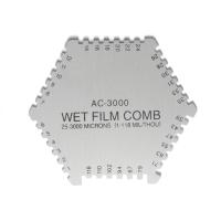
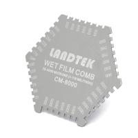
- 5How to measure film thickness with comb gauge?
- 6Thickness Wheel for thickness of wet film measurement
- 7What is wet-film and what is dry-film, and what is the relationship between the two?
- 8Spreader wet film thickness conversion