
LEEB230 F1 Coating Thickness Gauge with magnetic Induction F1 probe
 leeb230

Leeb leeb230 Coating Thickness GaugeSPEC
Leeb leeb230 Coating Thickness GaugeDetails
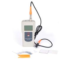
Leeb leeb230 Coating Thickness GaugePacking list
- SKU
- NB021714
- Measurement principle
- Magnetic Induction + eddy Current
- probe
- buy
- Interface
- USB
- Data storage
- 500 Measured values
- Power Supply
- 2 AAA alkaline batteries
- Display screen
- LCD backlight display
- Operating temperature
- 0~40℃
- Relative Humidity
- 20~90%RH
- Shell material
- Metal shell
- Voltage prompt
- underVoltage indication
- Machine Weight
- 350g
- Machine size
- 130*70*25mm

Using magnetic and eddy current measurement methods, it can non-destructively detect the thickness of the non-magnetic coating layer on the magnetic metal substrate (such as the steel alloy buckle is also better than the chromium, copper, zinc, tin rubber, paint, etc. on the steel), and the thickness of the non-conductive insulating coating on the non-magnetic metal matrix, such as aluminum, copper, zinc, rubber, plastic, paint, oxide film, etc.

Features
Automatic calibration of the zero point, the error can be modified systematically;
The upper and lower limits can be set to exceed the alarm
USB data transfer interface, which can be linked to a PC
Voltage prompt, automatic shutdown
Large LCD backlit display with adjustable contrast
Two-point calibration for improved accuracy
Optionalprobe
| probe | F400 | F1 | F1/90 | F10 | N400 | N1 | CN02 | |||||
| Principle | magnetism | eddy | ||||||||||
| Measuring range (μm) | 0~400 | 0~1250 | 0~10mm | 0~400 | 0~12500 | 10~200 | ||||||
| Measurement accuracy in μm | A little calibration | ±[(1~3)%H+0.7] | ±(3%H+1) | ±(3%H+10) | ±(3%H+1) | ±(3%H+1.5) | H+1) | |||||
| Two-point calibration | ±(1~3%H+0.7) | H+1] | ±[(1~3)%H+10] | ±[(1~3)%H+1] | ±[(1~3)%H+1.5] | --- | ||||||
| Low resolution | 0.1 | 0.1 | 1 | 0.1 | 0.1 | 1 | ||||||
| Minimum radius of curvature (mm) | (convex)1 | 1.5 | Straight | 10 | 1.5 | 3 | Flat surface only | |||||
| Minimum Area Diameter (mm) | Φ3 | Φ7 | Φ40 | Φ4 | Φ5 | Φ7 | ||||||
| Basic Critical Thickness (mm) | 0.2 | 0.5 | 2 | 0.3 | 0.3 | Unlimited | ||||||
Selection reference
| Cover matrix | Non-magnetic overlays such as organic materials (e.g. lacquer, lacquer, enamel, enamel, plastic, anodizing, etc.) | Non-magnetic non-ferrous metal overlays (e.g. chromium, zinc, aluminum, copper, tin, silver, etc.) | |||
| The thickness of the covering layer does not exceed 100 μm | The thickness of the overburden is more than 100 μm | The thickness of the covering layer does not exceed 100 μm | The thickness of the overburden is more than 100 μm | ||
| Such as iron, steel and other magnetic metals | The diameter of the measured area is greater than 30mm | F400 probe 0~400μm | Type F1 probe | F400 probe 0~400μm | Type F1 probe |
| Type F1 probe | 0~1250μm | Type F1 probe | 0~1250μm | ||
| 0~1250μm | Probe type F10 | 0~1250μm | Probe type F10 | ||
| 0~10μm | 0~10μm | ||||
| The diameter of the measured area is less than 30mm | F400 probe 0~400μm | F400 probe 0~400μm | F400 probe 0~400μm | F400 probe 0~400μm | |
| Type F1 probe | Type F1 probe | ||||
| 0~1250μm | 0~1250μm | ||||
| Such as copper, aluminum, brass, zinc, tin and other non-ferrous metals | The diameter of the measured area is greater than 10mm | N1 probe 0~1250μm | Only for chrome-plated N1 probe 0~40μm on copper and 0~40μm N400 probe | ||
| N400 probe 0~400μm | |||||
| The diameter of the measured area is greater than 10mm | N400 probe 0~400μm | N400 probe 0~40μm | |||
| Plastic, printed circuit non-metallic matrix | The diameter of the measured area is greater than 7mm | -- | -- | CN02 probe 10~200μm | |